“For the last year or so I’ve been using a Trion Orion PECVD at the University of Alberta Nanofab to deposit and control the stress and composition of silicon carbonitride (SiCN). The paper with my results is published in the Jan/Feb 2007 issue of JVST B 25(1), “Low-stress silicon carbonitride for the machining of high-frequency nanomechanical resonators”. I’ve also presented this work at conferences of the course of the project.
I also regularly use the Trion Phantom RIE to etch the SiCN. I’ve found both machines to be quite robust, indestructible by comparison to some other lab equipment. Here are some pictures of the resonant structures I’ve made using both the PECVD and RIE. One of the images has made it onto the 2006 Raith calendar (October). I’ve made functional resonators as thin as 50nm, and shown that they are indeed on par with Si resonators, as well as many others.
I work under Stephane Evoy, a professor in the ECE Department of the University of Alberta, who is also cross-appointed with the National Institute for Nanotechnology (NINT), the new national research facility that opened in Edmonton. At NINT we’re known as the Nanodevices and Sensors Group.
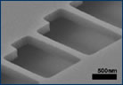
All pictures are of 200nm thick SiCN, except for JVST Fig 4. which is 50nm thick, and actually resonated (Q ~ 26 000).”
— Lee M. Fischer
National Institute for Nanotechnology
University of Alberta
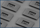
File 08: 200nm thick SiCN. An array of the experimental geometry resonators. (Courtesy Lee M. Fischer, NINT)
File 10: 200nm thick SiCN. Same as File 08. (Courtesy Lee M. Fischer, NINT)
JVST Fig 4: 50nm thick x 800nm wide beams, these are the ones measured in the paper* to examine the effects of stress. (*Jan/Feb 2007 issue of JVST B 25[1], “Low-stress silicon carbonitride for the machining of high-frequency nanomechanical resonators”). (Courtesy Lee M. Fischer, NINT)
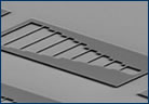
Small Bridges 1: 200nm thick x 200nm wide beams of SiCN. (Courtesy Lee M. Fischer, NINT)
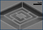
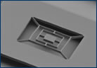
Suspend 2: 200nm thick SiCN. a multi-mode resonant structure used as a lithography and etching test (experimental geometry). (Courtesy Lee M. Fischer, NINT)
TWO NEW PAPERS!
(1) Poly-Si TFT Fabricated at 170 Degrees Celcius Using ICP-CVF and Excimer Laser
Annealing for Plastic Substrates
Read the full article >>
(2) P-13: Poly-Si TFT Fabricated at 170 Degrees Celcius Using ICP-CVF and Excimer Laser Annealing for Plastic Substrates
Both papers by: Seoul National University, research done in conjunction with Samsung
Application: Low temperature deposition consisting of both amorphous silicon AND SiO2
deposited with the ICP
Trion tool: ICP-equipped PECVD system
Read the full article >>
Application Note for Low Stress Nitride Deposition
Trion Tool: Oracle triode system
“The deposition of silicon nitride by silane (SiH4) and ammonia (NH3) can be summarized by the chemical reaction below …”
Read the full article >>
PAPER: Low-Stress Silicon Carbonitride for the Machining of High-Frequency Nanomechanical Resonators
By Lee M. Fischer, Neal Wilding, Murat Gel, and Stephane Evoy (University of Alberta)
Application: Deposition, MEMS
Trion Tool: Phantom RIE; Orion PECVD
read online here at avspublications.org
PAPER: Surface Characterization of Si02 – Decorated Nafion Membranes
By: A.C. Tavares, V. Felice, C. Harnagea, A. Pignolet (INRS-Énergie, Matériaux et Télécommunications) and B. O’Grady (Trion Technology)
Application: Deposition
Trion Tool: Orion PECVD
“Surface modification of Nafion (DuPont) membranes is a promising approach to overcome the methanol cross-over of Direct Methanol Fuel Cells (DMFC). The basic principle consists of …” Read the full article >>
Oracle Plasma Etch & Deposition System

Orion III PECVD
Minilock-Orion III Loadlocked PECVD