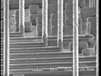
This process will etch thermal oxide, PECVD oxide, TEOS oxide, PSG and BPSG at rates of >1000 Å /min. The process is highly ion driven, and is well suited for anisotropic removal of inter-level dielectrics during failure analysis.
The silicon nitride etch process is more chemical in nature than the oxide etch process with an etch rate >1600 Å /min.
This process will etch Silicon using a SF6/O2 chemistry at an etch rate >4microns/min . Higher rates are possible if selectivity, or uniformity is not critical.

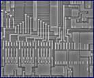
The delayering of all three samples was done by Chipworks using the Trion Phantom RIE.
Anisotropic Dielectric Removal vs. Sequential Removal
Application: Failure Analysis; Dielectric Etching
Anisotropic Etching of Polymers
Application: Failure Analysis; Dielectric Etching; Silicon Etching
Trion Tool: Phantom RIE
Hybrid Reactors & Deep Oxide (Skeleton)
Application: Failure Analysis; Dielectric Etching; Silicon Etching ICP
Polyimide Etch
Application: Failure Analysis; Dielectric Etching; Silicon Etching
Trion Tool: Phantom RIE
Polysilicon Etch
Application: Failure Analysis; Dielectric Etching; Silicon Etching
Trion Tool: Minilock-Phantom RIE
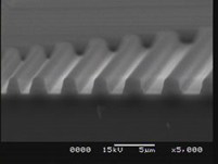
RIE Grass
Application: Failure Analysis; Dielectric Etching; Silicon Etching
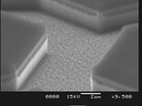
Silicon Dioxide Etch
Application: Failure Analysis; Dielectric Etching; Silicon Etching
Trion Tool: Phantom RIE
Silicon Nitride Etch
Application: Failure Analysis; Dielectric Etching; Silicon Etching
Trion Tool: Phantom RIE
Amorphous silicon thin-film transistors with 90° vertical nanoscale channel
by Isaac Chan and Arokia Nathan
Application: Failure Analysis, Dielectric Etching, Silicon Etching
Trion Tool: Phantom RIE
Planar Deprocessing Of Advanced VLSI Devices by K. Wills, Texas Instruments
Application: Failure Analysis; Dielectric Etching; Metal Etching Copper
Plasma Delayering of Integrated Circuits
by A. Crockett and M. Almoustafa (Trion Technology) and W. Vanderlinde (Laboratory for Physical Sciences, College Park, MD)
Application: Failure Analysis; Dielectric Etching; Silicon Etching
Rapid Integrated Circuit Delayering Without Grass
By W. Vanderlinde and C. Von Benken (Microelectronics Research Laboratory, Columbia, MD) and A. Crockett (Trion Technology)
Application: Failure Analysis; Dielectric Etching; Silicon Etching
Trion Tool: Minilock-Phantom RIE
Reliability Issues And Advanced Failure Analysis Deprocessing Techniques For Copper/Low-K Technology by H. Wu, J. Cargo, C. Peridier and J. Serpiello (Agere Systems, IC Quality Organization, Product Analysis Lab, Allentown, PA)
Application: Failure Analysis; Dielectric Etching; Metal Etching Copper
Trion Tool: Phantom RIE