750th machine ships.
750th machine ships.
550th machine ships.
550th machine ships.
Clearwater, FL, USA, February 21, 2013 -Trion Technology, manufacturer of plasma etch, strip and deposition systems for critical surfaces in the semiconductor and related industries, today announced a strategic alliance with European distributor, S3 Alliance. S3 Alliance will distribute and support Trion’s full line of products to customers throughout Europe.
S3 Alliance provides Trion Technology further penetration into the European market with an installed service and support network. Trion’s products expand S3 Alliance market offerings to the European customer base.
“We are pleased to be working with Trion Technology” stated Thomas Riedel, Managing Director of S3 Alliance GmbH. “They have a strong product range for production descum and photoresist removal and have extensive experience with RIE etching, ICP and microwave plasma generation as well as for PECVD. Trion products are perfectly enhancing our portfolio for our common targeted markets.
“We have contacted most of the existing European customers and have had only positive feedback,” commented Thomas Riedel. S3 Alliance will be working with R&D, MEMS and Production Fabs. Key accounts include major companies in the semiconductor industry, government research, universities, and research and development laboratories.
“This alliance demonstrates Trion’s continued dedication to providing world-class customer service and support,” stated Randy Crockett, President of Trion Technology. “We believe that providing highly responsive service is an essential factor in making our customers happy,” he continued.
About Trion: Founded in 1989, Trion Technology, Inc. of Clearwater, FL, USA supplies a variety of plasma etch and deposition equipment for the manufacturing of compound semiconductors and MEMS. Trion’s products feature the smallest footprint and lowest cost systems in the industry with proven production reliability. For more information: www.triontech.com
About S3 Alliance: S3 Alliance is a European trading and service company with a diversified product portfolio in the semiconductor and related industries. For more information: http://www.s3-alliance.com/
Click Here to Close
Clearwater, FL, USA, July 10, 2009 – Mr. Addison Crockett, founder of Trion Technology, a manufacturer of plasma etch, strip and deposition systems for critical surfaces in the semiconductor and related industries, is interviewed shortly before the commencement of SEMICON West 2009:
Can you speak about your company’s experience and expertise in the semiconductor industry?
This is Trion’s 20th year anniversary and we have been a debt free and profitable company that entire period. Trion began as a premier manufacturer of small laboratory and failure analysis plasma etch and deposition equipment. Also, it has been one of the few companies willing to design custom equipment. Within the past several years, we have successfully transitioned into a supplier of low cost production equipment in the photonics and compound semiconductor markets.
Can you talk about the products/services you will be showcasing at SEMICON 2009?
Of the various system types that we produce, we are showcasing our production resist stripper, the Apollo and our production etch platform, the Titan. Both of these systems have very small footprints and cost of ownership. The common philosophy behind all our systems is simplicity. Both of these platforms are currently in production facilities around the world.
Can you define and explain for us the specific applications for your products offerings?
As I discussed earlier, the Apollo is predominantly used as a resist stripper. But it also has applications wherever low device damage is essential. The Titan has been designed and characterized for the production of advanced photonics and compound semiconductor. Specifically, the etch of GaN, Quantum wells and structures for the manufacture of high brightness LEDs. Within the III-V market the system is capable of the etch and deposition of various layers used in RF power devices currently used in telecommunication.
Can you discuss how your company’s products and services fit in to the current challenging economic landscape – why they make economic sense today and in the coming years?
Over the years, semiconductor equipment has continuously grown in size, complexity and price. This is not Trion’s philosophy. We have been successful in keeping our systems small, simple and economic without sacrificing technology. This allows the users in emerging markets to afford new equipment when they would otherwise be forced to purchase old, obsolete systems from the used market. By keeping the designs simple, Trion offers its customers the competitive advantage of upgrading their fabs with state-of-the-art technology at an affordable cost. This is essential in this uncertain economic environment.
For more information about Trion Technology, visit www.triontech.com.
Click Here to Close
Clearwater, FL, USA, July 11, 2008 – Trion Technology, manufacturer of plasma etch, strip and deposition systems for critical surfaces in the semiconductor and related industries, is pleased to announce the sale of a further four of its Titan production platforms to a world leader in the high brightness LED marketplace.
The Titan is a compact fully automated vacuum cassette platform capable of batch processing of substrates from 2” through to 4” and of single wafers from 4” to 12”. The Titan is available in either Reactive Ion Etch (RIE) configuration, High Density Inductive Coupled Plasma (HDICP) or Plasma Enhanced Chemical Vapor Deposition (PECVD) configuration. The small system width provides very high throughput per linear foot in the fab.
Trion has a fully equipped laboratory for process support both prior to and subsequent to purchase. For a more detailed discussion, or for sales and service representatives worldwide, please visit www.triontech.com/contact/.
Trion opens Taiwanese Service Office.
Trion opens Taiwanese Service Office.
400th machine ships.
400th machine ships.
At SEMICON Europa 2007, Trion introduces the Gemini: a new multi-chamber photoresist stripper.
At SEMICON Europa 2007, Trion introduces the Gemini: a new multi-chamber photoresist stripper.
Clearwater, FL, USA, Tuesday, August 7, 2007 – Trion Technology announces the sale of multiple dual-chamber strippers for advanced packaging to Advanced Chip Engineering Technology, Inc. (ACET) of Taiwan. The systems will be used for the removal of polymers used within the advanced packaging of semiconductor devices.
Graham Muir, Trion’s VP Sales, stated: “We are very pleased to be chosen as a supplier of choice to ACE. The compact design of the Trion stripper fits neatly into the cost of ownership requirements of advanced packaging and in combination with the excellent services of our local representative Jetel Co., Inc., we are confident of continued success in this market in Taiwan.”
“About Trion: Founded in 1989, Trion Technology Inc of Clearwater, FL, USA supplies a variety of plasma etch and deposition equipment for the manufacturing of compound semiconductors, MEMS, and optoelectronics. Trion’s products feature the smallest footprint and lowest cost systems in the industry with proven production reliability.
About ACE: Established in 2000, Advanced Chip Engineering Technology Inc. (ACET) is a leading technologies company that integrates IC back-end manufacturing processes by using wafer level processes. They focus on the development and manufacturing of wafer level packaging, testing, burn-in and assembly etc. ACET own the technologies and patents on the wafer level packaging, wafer level burn-in circuit, wafer level probe card for final testing and new type burn-in socket for CSP/BGA package. ACET has strong teams on both the development and manufacturing in IC semiconductor field that provide excellent service to their customers.
Click Here to Close
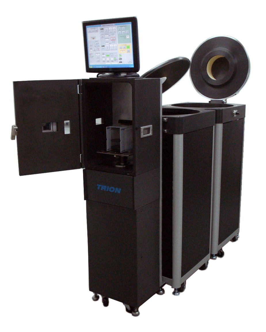 At SEMICON West 2007, Trion introduces the Titan: a new vacuum loadlocked plasma system for semiconductor production.
At SEMICON West 2007, Trion introduces the Titan: a new vacuum loadlocked plasma system for semiconductor production.