1. Silicon Reactive Ion Etch (RIE)
2. Silicon RIE using Inductively Coupled Plasma (ICP)
3. Silicon Deep Reactive Ion Etch
Anisotropic Etching of Polymers
Application: Failure Analysis; Dielectric Etching; Silicon Etching
Trion Tool: Phantom RIE
Polyimide Etch
Application: Failure Analysis; Dielectric Etching; Silicon Etching
Trion Tool: Phantom RIE
Polysilicon Etch
Application: Failure Analysis; Dielectric Etching; Silicon Etching
Trion Tool: Minilock-Phantom RIE
RIE Grass
Application: Failure Analysis; Dielectric Etching; Silicon Etching
Silicon Dioxide Etch
Application: Failure Analysis; Dielectric Etching; Silicon Etching
Trion Tool: Phantom RIE
Silicon Nitride Etch
Application: Failure Analysis; Dielectric Etching; Silicon Etching
Trion Tool: Phantom RIE
Plasma Delayering of Integrated Circuits
by A. Crockett and M. Almoustafa (Trion Technology) and W. Vanderlinde (Laboratory for Physical Sciences, College Park, MD)
Application: Failure Analysis; Dielectric Etching; Silicon Etching
Rapid Integrated Circuit Delayering Without Grass
By W. Vanderlinde and C. Von Benken (Microelectronics Research Laboratory, Columbia, MD) and A. Crockett (Trion Technology)
Application: Failure Analysis; Dielectric Etching; Silicon Etching
Trion Tool: Minilock-Phantom RIE
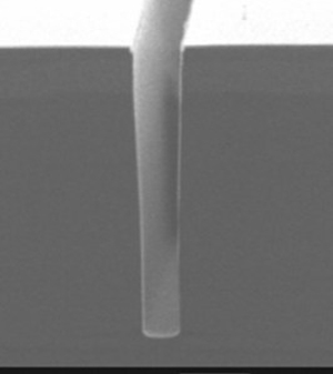
A TSV is a vertical electrical connection passing completely through the silicon wafer. The formation of this structure requires a highly anisotropic etch process, with silicon to resist selectivity high enough to allow for trenches with a depth of greater than 500µm. This non-switched process can achieve etch rates 10µm/min.
The process consists of two gasses that are active in the etching of silicon, the Etching Gas and the Passivation Gas, and can achieve etch rates over 10µm/min
Hybrid Reactors & Deep Oxide (Skeleton) Etch
Contamination resistant antireflection nano-textures in fused silica for laser optics
By Douglas Hobbs, Bruce MacLeod, Ernest Sabatino III from TelAztec LLC and Jerald Britten, Christopher Stolz from Lawrence Livermore National Laboratory
Application: Silicon RIE/ICP
Trion Tool: Phantom RIE/ICP
Hybrid Reactors & Deep Oxide (Skeleton) Etch
Application: Failure Analysis; Dielectric Etching; Silicon Etching ICP
Selective Reactive Ion Etching of P-Doped Polysilicon Using a Cl2/HBr Mixture
Trion Tool: Minilock-Phantom RIE
Controlled Multi-Batch Self-Assembly of Micro Devices by X. Xiong, University of Washington
Application: MEMS
Trion Tool: RIE
Double-Sided Micromachining Process for Silicon Cantilever Using a Parallel Capacitively Coupled Plasma by W. Wang, J. Ho, and P. Reinhall, University of Washington
Application: MEMS
Trion Tool: Phantom RIE
Fully Micromachined Power Combining Module for Millimeter-Wave Applications by Y. Lee, University of Michigan
Application: MEMS – Deep GaAs Etch
Trion Tool: RIE, Oracle Plasma Etch & Deposition System with Electrostatic Chuck and He Backside Cooling
Low-Stress Silicon Carbonitride for the Machining of High-Frequency Nanomechanical Resonators by L. Fischer, N. Wilding, M. Gel, and S. Evoy, University of Alberta
Application: Deposition, MEMS
Trion Tool: Phantom RIE; Orion PECVD
Micromachining of Non-Fouling Coatings for Bio-MEMS Applications by Y. Hanein, Y. Pan, B. Ratner, D. Denton, K. Bohringer, University of Washington
Application: MEMS
Trion Tool: RIE
Thermal Cycling Design Alternatives for the Polymerase Chain Reaction by M. Lewis, University of Maryland
Application: MEMS – Medical
Trion Tool: Minilock-Phantom RIE
Amorphous silicon thin-film transistors with 90° vertical nanoscale channel
by Isaac Chan and Arokia Nathan
Application: Failure Analysis, Dielectric Etching, Silicon Etching
Trion Tool: Phantom RIE