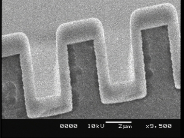
25.2e 4um wide trench with 2.4um thick SiO2 film
25a 2um wide trench with 1.7um thick SiO2 film
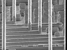
26b 4um
27a 2um
27b 4um
This process will deposit oxide at rates of >1000 Å /min.
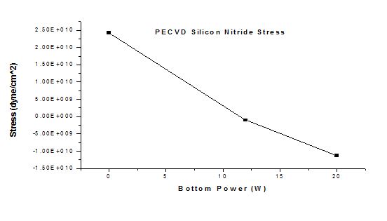
With 13.56 MHz top electrode, SiNx films based on a recipe of standard gases tend to be tensile where as with low frequency bottom electrode, which is usually below 1 MHz, the films tend to be compressive. A mix of both top and bottom power will result in low nitride films.
Minilock-Orion Loadlocked PECVD Tool
Orion PECVD Tool
“For the last year or so I’ve been using a Trion Orion PECVD at the University of Alberta Nanofab to deposit and control the stress and composition of silicon carbonitride (SiCN). The paper with my results is published in the Jan/Feb 2007 issue of JVST B 25(1), “Low-stress silicon carbonitride for the machining of high-frequency nanomechanical resonators”. I’ve also presented this work at conferences of the course of the project.
I also regularly use the Trion Phantom RIE to etch the SiCN. I’ve found both machines to be quite robust, indestructible by comparison to some other lab equipment. Here are some pictures of the resonant structures I’ve made using both the PECVD and RIE. One of the images has made it onto the 2006 Raith calendar (October). I’ve made functional resonators as thin as 50nm, and shown that they are indeed on par with Si resonators, as well as many others.
I work under Stephane Evoy, a professor in the ECE Department of the University of Alberta, who is also cross appointed with the National Institute for Nanotechnology (NINT), the new national research facility that opened in Edmonton. At NINT we’re known as the Nanodevices and Sensors Group.
All pictures are of 200nm thick SiCN, except for JVST Fig 4. which is 50nm thick, and actually resonated (Q ~ 26 000).”
– Lee M. Fischer, National Institute for Nanotechnology, University of Alberta
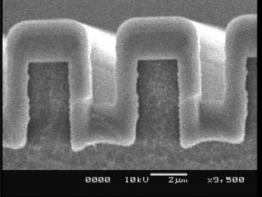
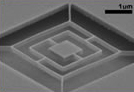
 File 08: 200nm thick SiCN. An array of the experimental geometry resonators. (Courtesy Lee M. Fischer, NINT)
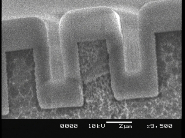
 File 10: 200nm thick SiCN. Same as File 08. (Courtesy Lee M. Fischer, NINT)
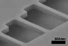
 JVST Fig 4: 50nm thick x 800nm wide beams, these are the ones measured in the paper* to examine the effects of stress. (*Jan/Feb 2007 issue of JVST B 25[1], “Low-stress silicon carbonitride for the machining of high-frequency nanomechanical resonators”). (Courtesy Lee M. Fischer, NINT)
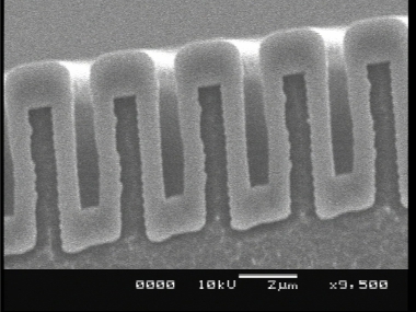
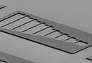
 Small Bridges 1: 200nm thick x 200nm wide beams of SiCN. (Courtesy Lee M. Fischer, NINT)
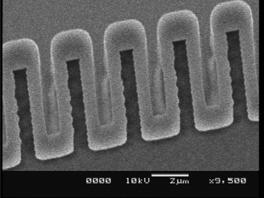
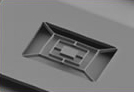
 Suspend 2: 200nm thick SiCN. a multi-mode resonant structure used as a lithography and etching test (experimental geometry). (Courtesy Lee M. Fischer, NINT)